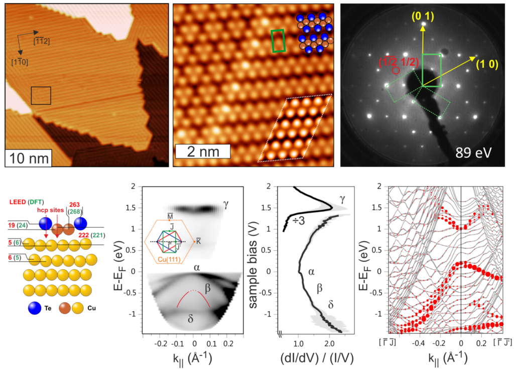
Combining the expertise of all groups at the chair of solid state physics we unraveled the structural and electronic properties of CuTe chains grown on Cu(111).
These chains form after the deposition of one-third of a monolayer of Te and a subsequent annealing step. They are extremely well ordered and cover the whole surface. By low-energy electron diffraction (LEED) intensity analysis, scanning tunneling microscopy (STM) and DFT we determine the structural parameters of this particular phase with picometer precision. Our analysis resolves long-standing discrepancies concerning this system found in literature. Using angle resolved photoemission spectroscopy (ARPES), the two-photon photoemission variant (AR-2PPE), scanning tunneling spectroscopy (STS) and DFT we explored the electronic properties of the CuTe chains. All relevant states could be identified with the employed methods and their electronic anisotropy was shown. One of the rare cases when science deals with “CuTe” chains.
Read all about it: Phys. Rev. B 102, 155422 (https://doi.org/10.1103/PhysRevB.102.155422) or https://arxiv.org/abs/2009.14618 (open access)