Advanced lab course experiments
Our chair offers several experiments within the scope of the advanced lab course in focus area C. Choose these experiments and get a first impression of experimental solid-state physics and surface science.

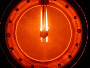
Low energy electron diffraction (LEED) is a well-established but still popular surface science method that has a long tradition in Erlangen. It is based on the first observations of low energy electrons diffraction patterns in the late 1927 [1] and the development of a useable surface science apparatus in 1960 [2]. Since then, LEED helped to resolve the surface atomic structure in an uncountable number of cases.
In this lab course, the students explore the adsorption of oxygen and nitrogen atoms on an tungsten (100) surface. For this they can use our state-of-the-art LEED optics developed at FKP and sold by companies nearly unchanged [3]. Furthermore, we give an introduction in the technique, handling and usage of an ultra-high-vacuum (UHV) chamber as well as experimental preparation techniques in UHV, like sample heating and controlled gas dosing.
[1]C. Davisson and L. H. Germer Phys. Rev. 30, 705 (1927)
[2] E. J. Scheibner, L. H. Germer, and C. D. Hartman, Rev. Sci. Instr. 31, 112 (1960)
[3] http://www.specs.de/cms/front_content.php?idcat=298 (access 13.08.18)
Contact

Scanning tunneling microscopy (STM) is one of the most important tools that can reveal the morphology and electronic states of conducting samples at the atomic scale in real space. In 1959, the “father” of nanoscience, Richard P. Feynman gave a visionary talk entitled “There’s Plenty of Room at the Bottom”. [1] He postulated the future world will go into the atomic scale, people will be able to “see” and “manipulate” atoms. 22 years later, his vision was put into action by Gerd Binnig and Heinrich Rohrer in IBM Zürich, who earned the Nobel prize in physics in 1986 for the invention of scanning tunneling microscopy [2] and finally in 1990 Don Eigler used the STM to spell the name of the little computer company that employed him with xenon atoms [3].
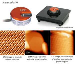
Here in this Lab course, students will learn the technics of a standard STM and operate a commercial STM (nanosurf [4]) to measure a clean graphite surface. Then, they will be instructed to use the knowledge from solid state physics and quantum mechanics to interpret their STM data, calculate the work function and plot density of state of graphite based on scanning tunneling spectroscopies (STS).
[1] http://calteches.library.caltech.edu/1976/
[2] G. Binnig, H. Rohrer, C. Gerber, and E. Weibel, PRL 49, 57 (1982)
[3] D. M. Eigler & E. K. Schweizer Nature 344, 524–526 (1990)
[4] https://www.nanosurf.com/en/products/naiostm-stm-for-nanoeducation
